The CSD25303W1015 is a P-Channel metal-oxide semiconductor field-effect transistor (MOSFET) is the most common type of field-effect transistor (FET). This transistor has a three-terminal device with Gate (G), Drain (D) and Source (S) terminals.
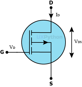
Circuit diagram symbol of the CSD25303W1015 transistor as follows.
| Transistor Code | CSD25303W1015 | |
|---|---|---|
| Transistor Type | MOSFET | |
| Control Channel Type | P-Channel | |
| Package | WLP1.0X1.5 | |
| Drain-Source Voltage (Maximum) | VDS | 20V |
| Gate-Source Voltage (Maximum) | VGS | 8V |
| Drain Current (Maximum) | ID | 3A |
| Drain-Source On-State Resistance (Maximum) | RDS(on) | 0.058Ohm |
| Power Dissipation (Maximum) | PD | 1.5W |
| Drain-Source Capacitance | 149pF | |
| Operating Junction Temperature (Maximum) | 150°C | |
| Rise Time | 8.6nS | |
| Gate-Threshold Voltage (Maximum) | 1V | |
| Total Gate Charge | 3.3nC | |
UXPython is not the creator or an official representative of the CSD25303W1015 MOSFET transistor. You can download the official CSD25303W1015 MOSFET transistor datasheet to get more infromation about this transistor.
Note : Copyrighted materials belong to their creator or official representative.

Copyright © UXPython inc. All rights reserved.
Devoloped by UXPython.