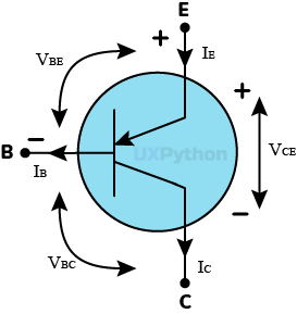
The CD93 is a bipolar junction transistor (BJT) with an PNP-type configuration. That means the CD93 transistor has a negatively charged layer between two positively charged layers. This transistor has three terminals Base, Collector, and Emitter.
The CD93 transistor symbol shows an arrow from the emitter into the base. This means that the current flows from emitter to collector terminal.
Circuit diagram symbol of the CD93 transistor as follows.
| Transistor Code | CD93 | |
|---|---|---|
| Transistor Type | BJT | |
| Transistor Polarity | PNP | |
| Transistor Material | Silicon(SI) | |
| Package | TO77 | |
| Collector Power Dissipation (Maximum) | PC | 0.4W |
| Collector-Base Voltage (Maximum) | VCB | 30V |
| Collector-Emitter Voltage (Maximum) | VCE | 30V |
| Collector Current (Maximum) | IC | 0.05A |
| Operating Junction Temperature (Maximum) | TJ | 175°C |
| Forward Current Transfer Ratio (hFE Value) | 50 | |
UXPython is not the creator or an official representative of the CD93 PNP transistor. You can download the official CD93 PNP transistor datasheet to get more infromation about this transistor.
Note : Copyrighted materials belong to their creator or official representative.

Copyright © UXPython inc. All rights reserved.
Devoloped by UXPython.